


The pretreatment process can significantly affect the corrosion resistance of electroless nickel (EN) coatings.
 Hong Deng and Per MollerOne of the most important reasons is that different pretreatment processes can give different surface morphologies of the substrate. The scanning electron microscope (SEM) and the scanning tunneling microscope (STM) have been used to investigate the structure and properties of EN coatings in the as-plated condition for various deposition times, in relation to different mechanical/chemical pretreatment processes.
The morphology of the substrate surface is found to be a key factor in control of the porosity of EN coatings. It can significantly affect the formation of EN deposits, not only in the early stage but also in the morphology/ structure during the continued growth of the deposit.
Possible porosity is associated with the morphology of the substrate and the coalescence of the nodules in the coating.
EIectroless nickel coatings are widely used because of their good corrosion and wear resistance. The ultimate success of electroless nickel plating depends on the selection of a suitable pretreatment process that determines the adhesion, morphology/structure and corrosion resistance of the coatings. Electroless nickel plating differs from other metal coating techniques because the substrate initiates the electroless chemical reduction process. Improper pretreatment can create passive spots that will not initiate electroless plating and that will result in non-uniform deposition, causing porosity. Because electroless nickel is a barrier coating, the absence of porosity is essential for good corrosion protection. The pretreatment process can significantly affect the corrosion resistance of the EN deposit.
Although the pretreatment process for electroless nickel plating requires the highest degree of care and control at all stages of the metal finishing procedure,1 it is probably the most easily overlooked aspect of the entire electroless nickel plating process; more attention is usually paid to the electroless nickel bath. Although the right type and best bath have been chosen, improper pretreatment can make the whole electroless nickel plating process fail.
The pretreatment processes for electroless nickel plating include mechanical/chemical cleaning, activation by acid and the pre-processing procedure. Many papers have been published on methods of cleaning the substrate, the constitution of the alkaline cleaning bath, and what type of acid should be chosen for activation, to increase the corrosion resistance of the subsequent electroless nickel coating.2-5 Evidence has been found showing that surface morphology is a key factor in maximizing corrosion resistance of subsequent electroless nickel deposits.6,7 The evidence indicated that the smoothest surface gave the best corrosion resistance. This conclusion is in accord with a recent report on ASTM program 14.8
In another paper by the authors, statistical methods were used to optimize the pretreatment process.9 Several types of mechanical treatment, polishing and pre-processing procedures (such as nickel strikes) were used to get different kinds of surface morphology. The experimental results from corrosion tests show that the surface morphology is a major controlling factor for the corrosion resistance of electroless nickel deposits.
Understanding the factors influencing the substrate surface morphology and its effects on the properties of the coating is essential for producing a high quality electroless nickel deposit. In this study, the scanning electron microscope (SEM) and the scanning tunneling microscope (STM) were used to investigate the morphology of the substrate surface and its effects on the structure and the properties of electroless nickel coatings in the as-plated condition at various deposition times.
Experimental Procedure
In these experiments, the substrate condition, the pretreatment processes and the electroless nickel plating bath condition were just the same as in our previous investigation.9 A highphosphorus (11 wt percent) electroless nickel commercial bath was used and the samples were plated at 89 to 90 “C in a magnetically stirred solution. The plating rate was constant at 12 µm/hr. The sample size was 20 x 20 mm for SEM and STM, and 100 x 150 mm for the SO2 moist corrosion test. The EN coating thickness for this test was 5 µm, and in the case of a bright nickel strike (1 µm), the EN coating thickness was 4 pm. The substrate was a low-carbon, cold-rolled steel, mechanically treated by one of the following methods: Grind l—the substrate surface was roughly ground with SiC stone; Grind 2— ground with SiC stone, but smoother; No Mechanical Treatment—the substrate was as delivered from the factory; Grit Blasting-the substrate was dry-blasted with glass bead; Water Blasting-the substrate was wet-blasted with glass bead. The substrate was also polished in two ways-chemical polishing and electropolishing in a commercial bath (about 3 µm thickness of the substrate was taken away by chemical polishing and electropolishing). In the pre-processing procedure, a bright nickel strike over the substrate surface was carried out in a commercial electrolytic bright nickel bath. The substrate samples used for tests had undergone the pretreatment process and were properly prepared for electroless nickel plating. The EN deposit samples for test were taken from the EN bath after a selected deposition time, rinsed and dried with air.
Table 1: Roughness of Substrates with Different Pretreatments
| Mechanical Treatment | Grind 2 | Grind 1 | No. Mech.1 | Grit Blasting | Water Blasting |
| Roughness Ra (µm) | 0.43 | 0.75 | 1.19 | 1.70 | 1.69 |
SEM and STM examinations were used for characterization of the surface. The surface roughness and the profile were measured with a stylus roughness meter.
Results and Discussion
Morphology of substrate surfaces after different mechanical treatments
The SEM pictures of the substrate surface after several kinds of mechanical treatment (Grind 1, Grind 2, Grit Blasting and Water Blasting) and no treatment are shown in Fig. 1, together with the surface profiles. The roughness of these substrate surfaces is listed in the table, and the corresponding corrosion resistance rating numbers9 are shown in Fig. 2. Figure 1 shows that the surface morphology is very dependent upon the different mechanical treatments. The surface of Grind 2, with the lowest Ra value, is full of small grinding marks (Fig. 1a). On the Grind 1 surface, the grinding marks are bigger and less uniform than those on the Grind 2 surface (Fig. 1 b). The surface with no mechanical treatment looked smoother and more uniform except for a few marks from the rolling (Fig. 1 c). After Grit Blasting and Water Blasting, the surface looks torn, rough and non-uniform; the structure of the surface seems badly damaged (Figs. 1 d and e). Although the Grit Blasting and Water Blasting surfaces have almost the same roughness, the Grit Blasting surface looks more torn. Figure 1 (a-e), the table and Fig. 2 show that the smooth and uniform substrate surface can give good corrosion resistance, and that the roughness parameters are insufficient to describe the morphology of the surface.
Morphology of substrate surfaces after polishing and nickel strike processes
The corrosion experiment results in Fig. 2 show that chemical polishing, electropolishing and a bright nickel strike (1 µm) can enhance the corrosion resistance of an EN deposit. The substrate for Grind 2 was taken as a case example to investigate the effect of chemical polishing, electropolishing and a bright nickel strike. Figure 3 shows the SEM pictures of substrate surface Grind 2 after chemical polishing, after electropolishing and after a bright nickel strike (1 µm). In Fig. 1a, it is shown that there are some peaks and troughs on the Grind 2 surface. After chemical polishing, the Grind 2 surface became very smooth, and the peaks were flattened, but some carbide particles remained on the surface (Fig. 3a). After electropolishing, the surface was very porous (Fig. 3b), but without micro-burrs. After a bright nickel strike (1 µm), the surface became comparatively smooth and the troughs filled with nickel because of the leveling ability of the bright nickel solution (Fig. 3c).
Effect of substrate morphology on the EN deposition process
Figures 1 (a-e) and 3(a-c) show that different pretreatment processes yield different surface morphologies of the substrate. The SEM pictures of Figs. 4-7 show how the surface morphology of the substrate affects the growth process of EN deposits, Figure 4 shows, respectively, the EN as-plated surfaces after 0, 1, 5, 10, 20, and 30 min of deposition on the Grind 2 substrate. Nickel deposition begins with a few isolated nodules (Fig. 4c); later, the nodules increase in number and grow (Fig. 4e), and still later, the growing nodules impinge on each other (Fig. 4f). In general, deposition of the nodules is along the grinding marks on the substrate, as observed by W.J. Tomlinson. 10
Figure 5 shows the deposit-growing process on the Grind 2 substrate after chemical polishing. After 1 rein, deposition of many small nodules of nickel are found on the surface (Fig. 5b); later, the nodules grow and very soon coalesce (Fig. 5d). New nodules emerge on top of the coalesced nodules (Fig. 5e) and these new nodules grow and coalesce again (Fig. 5f). This tendency is maintained during the entire deposition.
Figure 6 shows the SEM pictures of the EN as-plated surface after 0, 1, 5, 10, 20 and 30 min deposition, respectively, on the Grind 2 substrate after electropolishing. Deposition begins with many fine nodules on the porous substrate (Fig. 6c). These nodules grow and coalesce faster than on a chemically polished substrate and the nodules coalesce more tightly. After 10 min deposition, the structure of the deposit leads to an appearance resembling that of cauliflower (Figs. 6e and f), which becomes more and more compact as deposition progresses. In Fig. 7, the EN as-plated surfaces are shown after O, 1,5, 10, 20 and 30 min deposition, respectively, on the Grind 2 substrate after a bright nickel strike. Deposition begins uniformly over the entire surface and grows like a film (Fig. 7d), but small nodules of nickel are found on the surface (Fig. 7e). This pattern is still maintained after 30 min deposition (Fig. 7f).
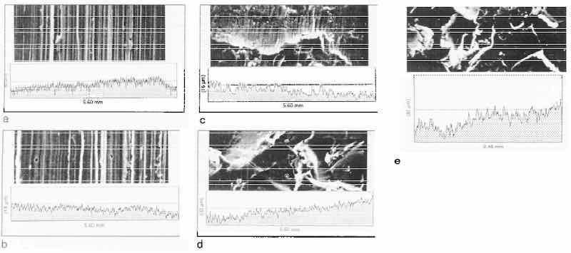
Fig. 1: SEM micrographs of substrate surface after mechanical treatment: (e) grind 2; (b) grind 1; (c) no treatment; (d) grit blasting; (e) water blasting.
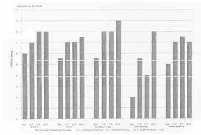
Fig. 2: Results of corrosion experiments with 5µm EN coatings under different pretreatment processes.
The SEM pictures in Figs. 4-7 show that the surface morphology does actually affect the deposition process of electroless nickel. It affects the formation of electroless nickel deposits in the early stage and affects the growth and porosity of the entire deposit as well. The more uniform the substrate surface, the more uniform the structure of the deposit, and the less porous the coating. These findings are consistent with the results from investigations using STM in situ.11,12 Although SEM can provide clear pictures of a surface, STM can offer resolution even on an atomic scale. Figures 8a and b show surface details not readily apparent with SEM.
The morphology/structure of the deposit, which dominates in determining the overall properties of the coating, is in fact established in the initial deposition stages. This conclusion is in accord with other investigations.13
Summary
The morphology of the steel substrate surface is a key factor in control of the porosity of electroless nickel deposits. Different pretreatment processes give different surface morphologies. Grit blasting methods to pretreat the steel surface before plating (Figs. 1 d and e) will reduce the possibility of obtaining EN coatings with low porosity. A fine grinding (Fig. 1a) with an Ra value of 0.43 µm is not as good as expected for the improvement of the quality of EN coating with respect to porosity, compared with the more rough-ground surface (Fig. 1 b) with an Ra value of 0.75 µm and the surface with no mechanical treatment (Fig. 1 c), with an Ra value of 1.19 µm. The resins show that roughness of the surface is not enough to describe the surface morphology properly.
Different chemical/electrochemical methods, such as chemical polishing and electrochemical polishing before plating will reduce or eliminate micro-burrs on the mechanically treated surfaces (Fig. 3). These treatments seem to improve the quality of the EN deposit significantly with respect to porosity (Fig. 2). The effect of these pretreatments is especially obvious at the grit-blasted substrate surfaces with many micro-burrs (Fig. 1 d).
An especially bright nickel strike (1 pm) over the substrate before EN plating has a good leveling effect and can significantly improve the quality of the EN coating with respect to porosity. The effect of the bright nickel strike is obvious from the corrosion experiment results (Fig. 2) for the case of grit blasting of the steel surface, followed by a bright nickel strike (1 µm) and EN deposit (4 µm). Other types of nickel strike, such as sulfamate nickel, give no improvement of the quality of EN coatings. Woods nickel and semi-bright nickel strike show some improvement in the quality of EN coatings, but not so much as a bright nickel strike.
A substrate surface, both chemically and topographically uniform, has a better chance for a pore-free EN coating. For example, a bright Ni strike before EN plating, which can make the substrate surface more smooth and chemically uniform (Ni on the surface), can improve the corrosion resistance of the EN coating significantly.
An investigation of the deposition process of EN coating on different steel substrate surfaces (Figs. 4-7) shows that the morphology of the substrate affects the formation of EN deposits not only in the early stages but later, during the continued growth of the deposits as well. This seems to explain the large differences in porosity of EN coatings deposited on different substrate surfaces.
The investigations show that the conventional roughness measurements of surfaces are not able to give the necessary information about the EN-platability of substrate surfaces. Perhaps in the future, new methods, such as STM, will make it possible to give a more precise description of the substrate surface, and make it possible to predict the quality of an EN coating for a particular substrate morphology.
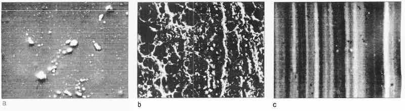
Fig. 3: SEM micrographs of Grind 2 substrate surface: (a) with chemical polishing; (b) with electrolytic polishing; (c) with bright nickel strike.
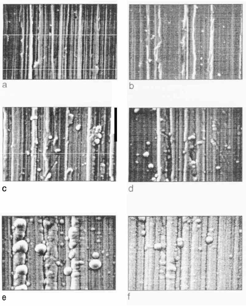
Fig. 4: EN as-plated surfaces of Grind 2 substrate after various deposition times: (a) O min; (b) 1 min; (c) 5 min; (d) 10 min; (e) 20 min; (f) 30 min.
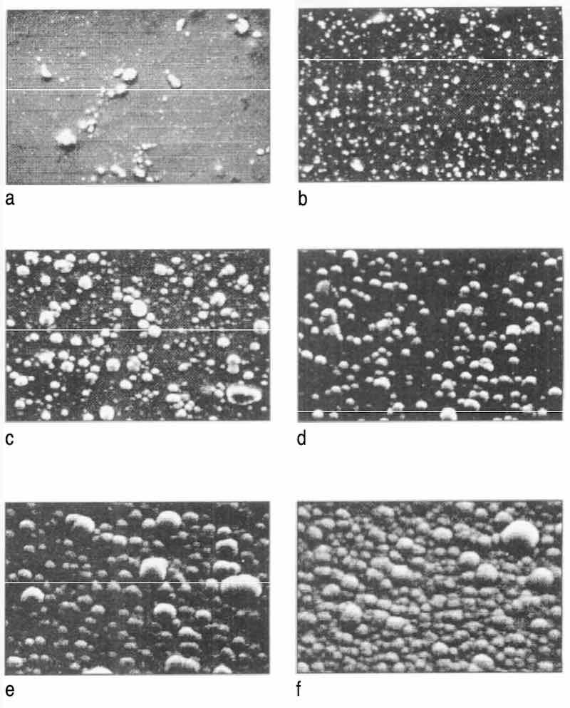
Fig 5: Progress of EN deposition on Grind 2 substrate after chemical polishing and deposition rate of 12 µm/hr: (a) O rein; (b) 1 rein; (c) 5 rein; (d) 10 rein; (e) 20 mm; (f) 30 min.
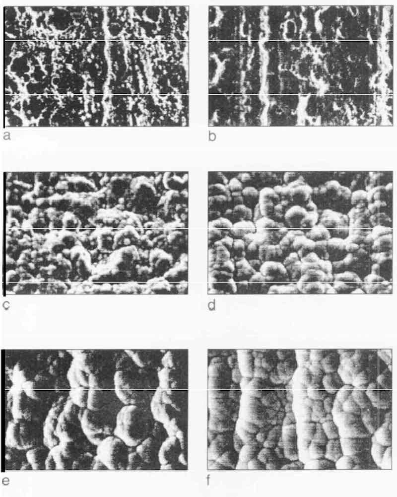
Fig. 6—Progress of EN deposition on Grind 2 substrate after electropolishing and deposition rate of 12 µm/hr: (a) O rein; (b) 1 rein; (c) 5 rein; (d) 10 rein; (e) rein; (f) 30 min.
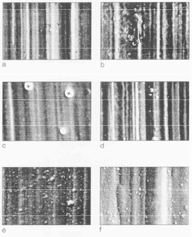
Fig. 7—Progress of EN deposition on Grind 2 substrate after bright nickel strike and deposition rate of 12 µm/hr: (a) O min; (b) 1 min; (c) 5 min; (d) 10 min; (e) 20 rein; (f) 30 min.
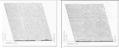
Fig. 8: STM images of Grind 2 substrate surface: (a) as-delivered; (b) with chemical polishing.
Note: This paper was published in 1994.
About the Authors
Dr. Hong Deng is a researcher at the Centre of Advanced Electroplating of the Technical University of Denmark, Bldg. 425, DK-2800, Lyngby, Denmark. She holds a BS in applied chemistry and an MS in chemical engineering from Dalian University of Technology (China) and a PhD in plating and surface finishing from the Technical University of Denmark. Dr. Per Moller is director of the Centre of Advanced Electroplating, Technical University of Denmark. He received his PhD in electroplating from the Technical University of Denmark. He is a member of the European Academy of Surface Technology (EAST).
References
- G.O. Mallory, and J.B. Hajdu, Electroless Plating, American Electroplates and Surface Finishers Society, Orlando, FL, 1990.
- L.J. Durney, Electroplating Engineering Handbook, 4th Ed., Van Nostrand Reinhold, New York, 1984.
- ASTM B656-86, “Standard Guide for Autocatalytic NickelPhosphorus Deposits on Metals for Engineering Use.”
- ASTM B322-68, “Standard Practice for Cleaning Metals Prior to Electroplating.”
- C.F. Beer, Surface Tech. 12,89(1981).
- J.A. Johnson and H.L. Morris, Proc. Electroless Nickel Conf. II, 1980.
- M.J. Coussement, P. Jansen, J.R. Roos, J.P. Celis and M. Neutjens, Proc. Electroless Nickel Conf. IV, 1985.
- G. DiBari, Proc. Electroless Nickel Con f., 1991.
- H. Deng and P. Moller, Proc. AESF SUR/FIN International ’92, Session O, Atlanta, 1992.
- W.J. Tomlinson and J.P. Mayor, Surf. Engineering, 4(3), 235 (1988).
- W. Richtering and K-H. Pietsch, British Electroless Nickel Society: Proc. Electroless Nickel Conf., Corwen, Clwyd, UK (1991).
- T. Homma, T. Tamazaki, T. Kubota and T. Osaka, J. Applied Physics (Japan), 29, L2114 (Nov., 1990).
- H. Matsubara, M. Toda, T. Sakuma, T. Homma, T. Osaka, T. Yamazaki, and T. Namikava, J. Electrochem. Soc., 136, 753 (1989).